Intel Bets $5 Billion on Singapore: Why Advanced Packaging Becomes the New Hotspot for Chip Investment?
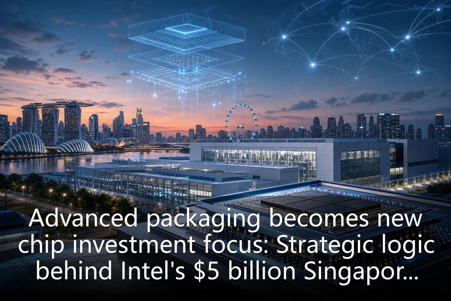
On July 28, 2026, Intel officially announced the start of construction for an advanced packaging plant at Singapore's Tampines Wafer Park, with a total investment of $5 billion, expected to begin mass production in 2028, primarily serving AI accelerators, data centers, and high-end IoT chips. This move is not only a key step in Intel's Asia-Pacific strategy but also reveals a profound shift in global semiconductor investment logic — as advanced process nodes approach physical limits, advanced packaging technology is becoming a new engine to enhance chip performance and extend Moore's Law.
1. Why Has Advanced Packaging Become a New Investment Focus?
Moore's Law slowing down is an indisputable fact. TSMC and Samsung face increasingly severe yield and cost challenges at nodes below 3nm, leading to diminishing cost-performance gains per generation. Instead of solely pursuing line width reduction, the industry is turning to 2.5D/3D stacking, heterogeneous integration, silicon bridges and other advanced packaging technologies to tightly integrate different functional dies, achieving higher performance, lower power consumption, and smaller form factors. According to the Semiconductor Industry Association (SIA), the global advanced packaging market is expected to exceed $60 billion in 2026, with a compound annual growth rate of 18%, far outpacing the overall semiconductor market's 8%.
Intel's Strategic Considerations for Choosing Singapore
Intel CEO Pat Gelsinger stated in the announcement that Singapore boasts a stable political environment, robust intellectual property protection, abundant supply of high-end talent, and close ties with the Southeast Asian semiconductor supply chain. In fact, Singapore already hosts production bases for the world's top five packaging and testing firms (ASE, Amkor, JCET, etc.), forming a mature packaging ecosystem. Intel's entry will further enhance Singapore's global influence in advanced packaging and drive investment opportunities across upstream and downstream equipment, materials, and design services.
2. Three Major Trends in the Chip Industry From Intel's Investment
Trend 1: AI Chip Demand Drives Packaging Technology Upgrades
Training and inference of large AI models require massive computing power, and traditional single-chip solutions face memory bandwidth and power wall bottlenecks. For example, NVIDIA's H100 uses TSMC's CoWoS (Chip-on-Wafer-on-Substrate) technology to vertically stack GPU and HBM memory, achieving data transfer rates up to 2TB/s. Intel's new Singapore plant will focus on Foveros Direct and EMIB technologies, targeting 3D packaging for AI chips, expected to serve its Gaudi series and external customers.
Trend 2: Supply Chain Localization and Risk Diversification
Geopolitical risks are driving global chip supply chains from concentration to dispersion. The US CHIPS Act and EU Chips Act heavily subsidize domestic manufacturing, but advanced packaging capacity remains highly concentrated in Taiwan (TSMC) and South Korea (Samsung). By deploying packaging capacity in Penang, Malaysia; Arizona, USA; and Ireland, along with the new Singapore plant, Intel creates diversified supply nodes to mitigate single-region disruption risks.
Trend 3: Localization Opportunities for Packaging Equipment and Materials
China's goal of increasing semiconductor self-sufficiency is driving a wave of localization for packaging equipment and materials. Temporary bonders, laser cutters, ABF substrates required for advanced packaging are currently dominated by a few players like Japan's Disco, US Applied Materials, and Taiwan's Kinsus. However, Chinese local companies such as Shanghai Micro Electronics and Deyang Laser have achieved breakthroughs in some segments, creating new investment hotspots. Investors can focus on targets related to advanced packaging equipment, testing, and substrates.
3. Investment Recommendations and Risk Warnings
Key Areas to Watch
- Packaging and testing foundries: ASE, Amkor, JCET are among the first to benefit from advanced packaging demand growth;
- Equipment suppliers: Applied Materials, Tokyo Electron, KLA hold technology moats in semiconductor packaging equipment;
- Substrates and materials: Japan's Toppan Printing, Taiwan's Unimicron, Japan's Ajinomoto are expanding ABF substrate capacity;
- Design service companies: Firms like VeriSilicon, Arteris that provide advanced packaging design solutions for AI chips.
Risk Factors
Advanced packaging investments are long-cycle and fast-iterating; the following risks need attention:
• Divergent technology roadmaps (e.g., TSMC's CoWoS vs Intel's Foveros) could lead to a shakeout;
• Fluctuations in end demand; if AI capital expenditure slows, it will directly impact packaging capacity utilization;
• Escalating geopolitical tensions may restrict exports of certain equipment and materials.
Conclusion
Intel's Singapore expansion is a microcosm of the global semiconductor industry's tilt toward advanced packaging. For investors, chip investment is no longer solely focused on advanced process nodes; advanced packaging is opening a second growth curve. Seizing the three major themes of heterogeneous integration, AI-driven demand, and supply chain restructuring will enable one to gain an early advantage in the new wave of chip investment.